Modern B2B enterprises and cloud services require highly customized, robust networking paradigms to avoid localized bottlenecks. As a premier provider of Custom OEM HPE Networking integration solutions, we offer structural optimization, ASIC customization, and tailored optical transceiver modules configured to operate natively within HPE-centric ecosystems. Today's dynamic workload demands—spanning massive machine learning tasks, low-latency financial transactions, and distributed data lakes—make custom network topologies a strategic necessity rather than an operational convenience.
By partnering with specialized OEM manufacturing, global enterprises can design proprietary chassis configurations, adapt custom security architectures, and optimize power delivery systems. Through our deep industry alignment, we offer system engineering that guarantees hardware compatibility, high-density line rates, and full compliance with HPE's advanced orchestration interfaces. This guarantees that your customized architecture is ready to perform under peak utilization.
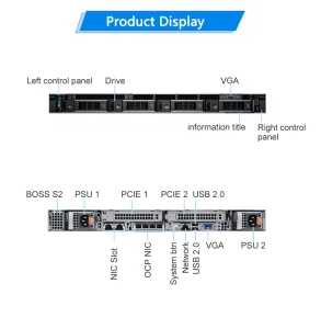
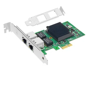
We optimize optical modules and switch interfaces for perfect firmware handshake matches with HPE FlexFabric, StoreFabric, and ArubaOS engines, preventing system warnings and dropped packets.
All custom boards feature custom crypto-processor chips that interface directly with HPE's Silicon Root of Trust, verifying firmware legitimacy before launching the operating system.
Tailored layout designs utilizing PCIe Gen5 buses and direct copper configurations (DAC) to lower trace lengths, bringing down end-to-end packet processing latency under 1 microsecond.
As a core division of our manufacturing cooperative, NexaGPU serves as a highly specialized AI GPU server and network hardware manufacturer, focusing on high-performance computing infrastructure, complex GPU clusters, and customized enterprise networking solutions. Since our founding in 2016, we have built a robust reputation for hardware precision, technical validation, and rapid customization workflows.
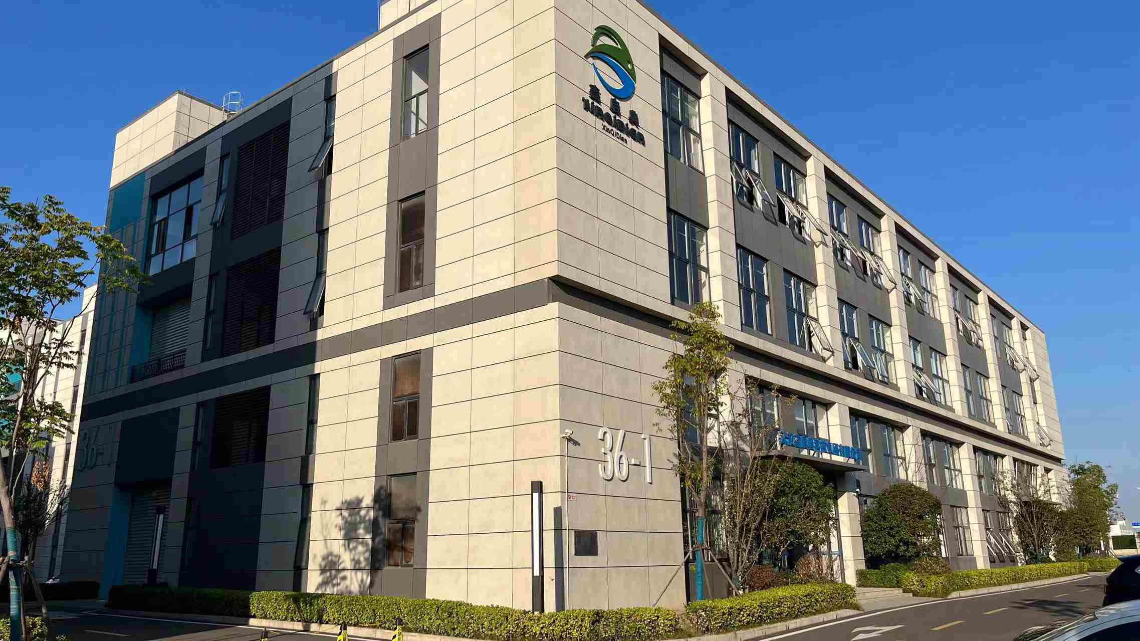
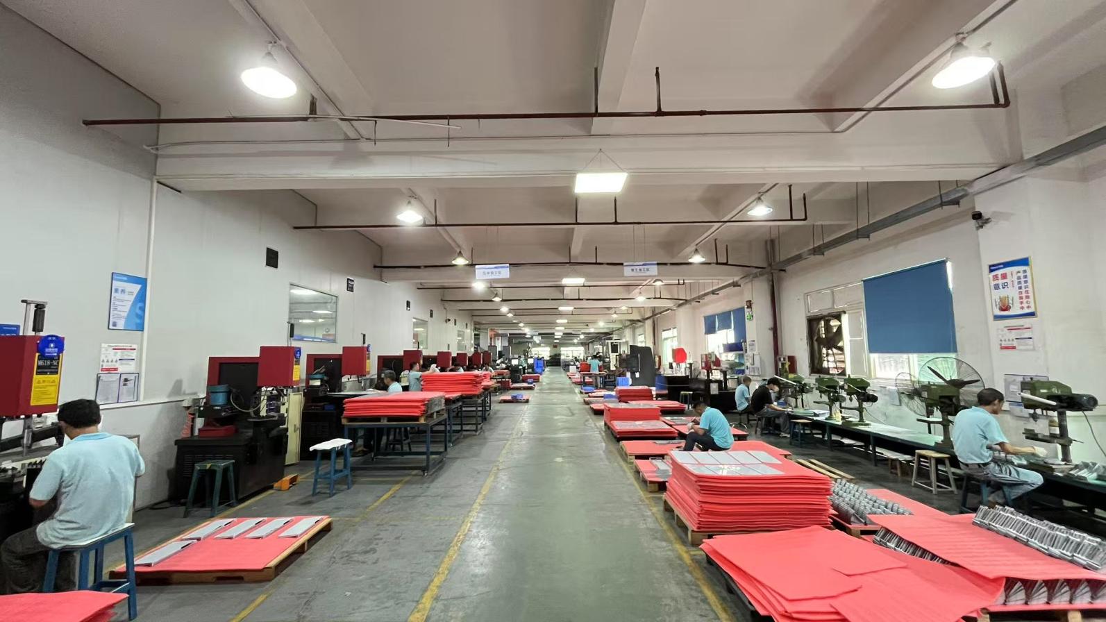
Operating from a modern manufacturing and testing facility with a dedicated building area of approximately 320㎡, we specialize in high-efficiency, multi-stage production and stress testing. This facility allows us to implement stringent hardware optimization policies. With 6 years of international B2B export experience, NexaGPU is uniquely positioned to handle localized customs, strict environmental declarations, and logistics across diverse global regions.
Our R&D pipeline is supported by a talented team of 120 dedicated R&D engineers whose specializations range from optical physics and thermal dynamic simulation to high-speed PCIe layer designs and liquid cooling loops. Over the past year, we have introduced 85 new product models, targeting deep learning, scale-out HPC clustering, and custom server systems designed to interface seamlessly with HPE ProLiant platforms.
Shenzhen and the surrounding Pearl River Delta area host the most complete, dense, and fast-moving electronics supply chains globally. We maintain close working relations with over 850 verified supply chain partners. This ecosystem provides us with direct, unfiltered access to essential sub-assembly components, customized metal fabrication for chassis, advanced thermal paste technologies, multi-layered PCB substrates, and top-tier chipsets.
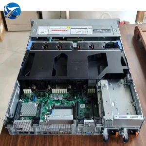
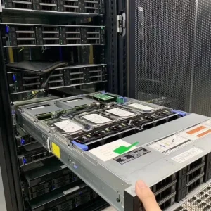
Every network adapter, controller card, and custom switch assembly undergoes a strict inspection lifecycle managed by our 45 specialized Quality Control (QC) officers. This includes automated optical inspection (AOI), x-ray structural analysis for micro-cracks, thermal cycling in environmental chambers, and high-frequency traffic stress testing.
Our tightly integrated manufacturing flow allows us to translate a technical specification document into a functional, bench-tested physical prototype within 14 business days. This fast turnaround minimizes time-to-market for modern data center operators deploying custom gear.
By maintaining strategic buffers of core microcontrollers, transceivers, and optical lenses, we protect our clients from global semiconductor supply shocks, ensuring reliable, continuous shipping schedules.
As workloads shift toward massive scale-out artificial intelligence training, networking architectures must scale alongside compute capacity. The emergence of model architectures like DeepSeek R1 671B requires ultra-low latency cluster fabrics. In order to support these models, we have developed a forward-looking product roadmap focused on extreme performance optimization.
| Technology Segment | Current OEM Standard | 18-Month Deployment Target | Primary Application Areas |
|---|---|---|---|
| Optical Transmission | 400G QSFP-DD Transceivers | 800G / 1.6T OSFP Co-Packaged Optics (CPO) | Hyperscale LLM Clusters, High-Performance Storage Arrays |
| Interface Bus | PCIe Gen 5.0 (32 GT/s per lane) | PCIe Gen 6.0 (PAM4 signaling, 64 GT/s) | Ultra-fast GPU-to-NIC routing, Direct Memory Access |
| Network Fabric | RoCE v2 & InfiniBand NDR (400G) | InfiniBand XDR (800G) & Ultra Ethernet Consortium (UEC) | Lossless distributed deep learning environments |
| Thermal Management | Air cooling & Closed-loop liquid cold plates | Two-Phase Immersion Cooling Integration | High-density containerized edge data centers |
Our engineering efforts focus on optimizing physical path traces. Over long physical lengths on PCBs, high-speed signals experience attenuation. By utilizing advanced low-loss dielectric substrate boards (such as Megtron 6/7) and optimizing layout tracing, our custom network solutions ensure minimal bit error rates (BER), maximizing the throughput of your HPE servers.
Our custom network integration options are designed for specific workloads across North America, Europe, Southeast Asia, and the Middle East:
In North American financial centers, microseconds determine transaction success. We supply customized OEM networking adapters optimized for sub-microsecond latency, allowing HPE ProLiant systems to capture financial feeds with minimal latency.
Large AI infrastructures deploying DeepSeek or Llama frameworks utilize clusters of specialized xFusion and HPE servers. We design customized Top-of-Rack (ToR) switches supporting RoCE v2 congestion avoidance protocols, avoiding packet loss during all-reduce steps.
For remote industrial locations, including offshore wind platforms in northern Europe or desert solar installations in the Middle East, standard networking gear can fail due to environmental factors. We manufacture fanless, dust-sealed, and temperature-hardened switches.
Entering international markets requires meeting complex regulatory frameworks. Every OEM network component we produce is certified to comply with relevant safety and environmental regulations:
Guarantees electromagnetic compatibility, preventing interference with surrounding computing equipment in high-density rack deployments.
Ensures lead-free and environmentally friendly materials, complying with strict European import requirements.
Tested within native HPE Active Health System frameworks, ensuring that diagnostics tools register the hardware correctly.
Uses approved semiconductor suppliers, ensuring compliance for public sector projects in North America.
Beyond regulatory compliance, we provide local warehousing options, direct SLA-backed support engineering, and firmware update support. This ensures that your customized hardware receives ongoing security and feature updates throughout its lifecycle.
We program our custom adapters and transceivers to comply with HPE's hardware identification protocols. During system boot, the server's UEFI and Integrated Lights-Out (iLO) systems identify the network components through programmed EEPROM signatures. This prevents the system warning flags or fan speed increases that often occur when non-certified third-party devices are detected.
Our flexible manufacturing approach supports a range of project sizes. While custom silicon/ASIC mask variations typically require larger quantities due to fabrication costs, standard modifications (such as custom PCB layouts, specialized EEPROM coding, tailored bracket designs, and customized thermal cooling blocks) can be developed with a low MOQ of 50 to 100 units.
Our QC team of 45 specialists manages a multi-stage testing process. This includes component inspection (microscope testing of raw silicon mounts), AOI testing post-SMT assembly, and a continuous 72-hour burn-in phase under thermal stress (50°C). We also run automated script testing at maximum packet loads (PRBS stress tests) to ensure zero frame loss, targeting a Field Defect Rate of under 0.05%.
We track component lifecycles closely and maintain end-of-life (EOL) strategies for our custom products. We stock buffer components for critical ICs to support long-term agreements, ensuring we can supply identical replacement units and provide hardware maintenance for up to 5-7 years.
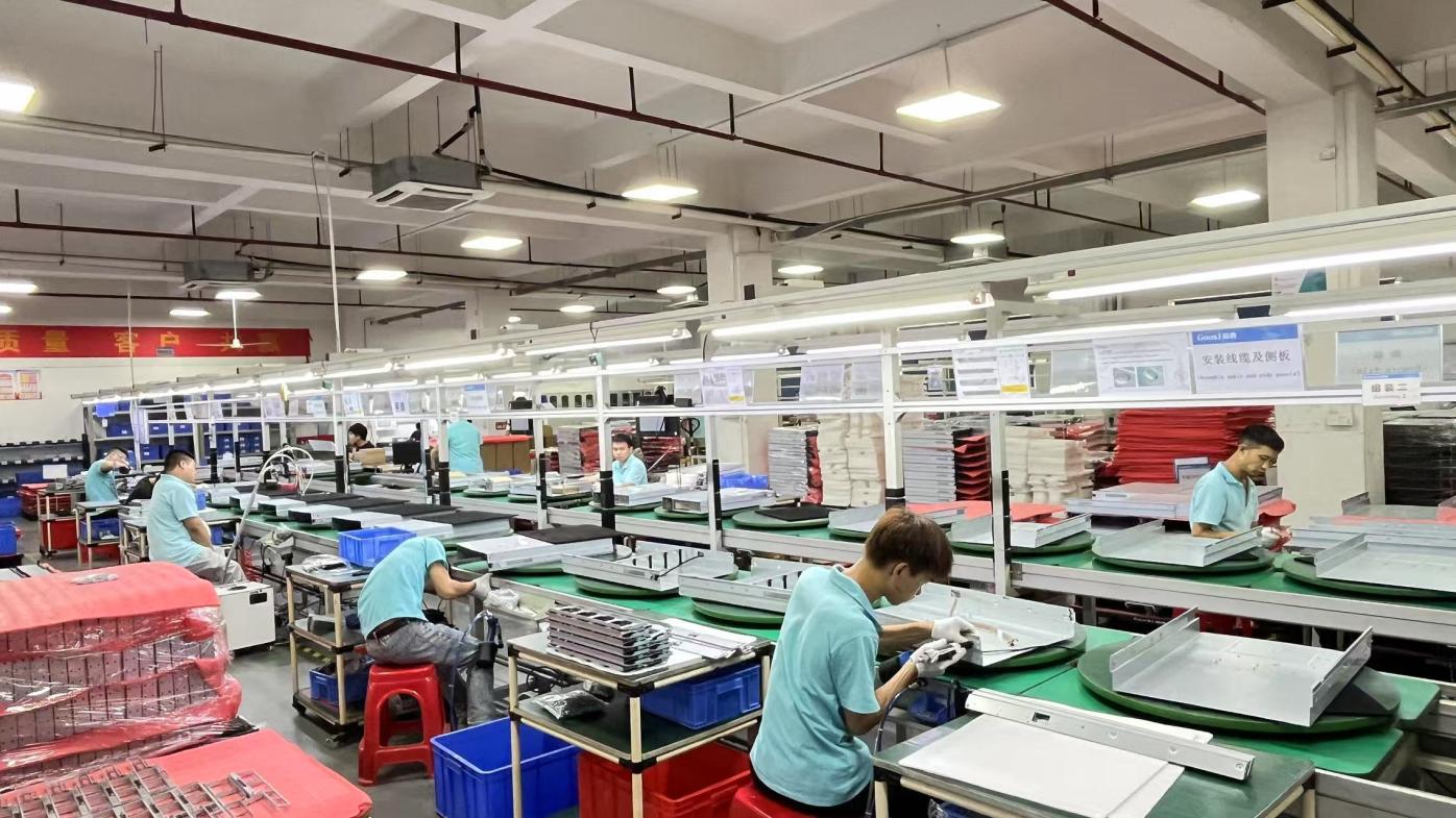
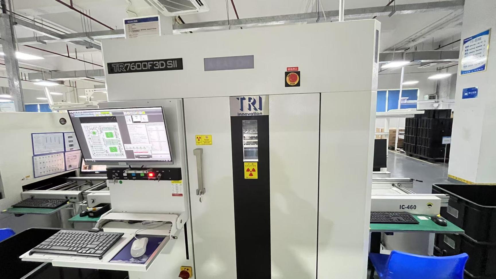
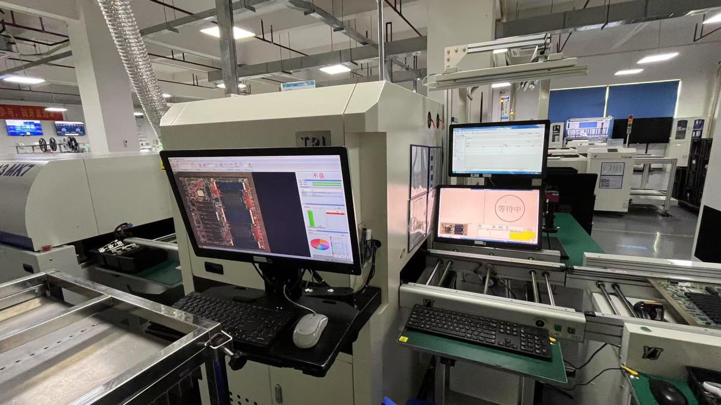
These verified photographs showcase our assembly spaces, thermal chambers, and testing floors. We ensure that our infrastructure meets strict international standards: