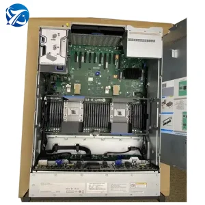
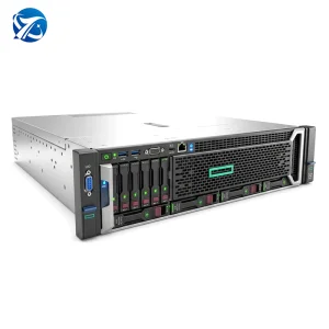
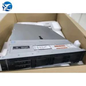
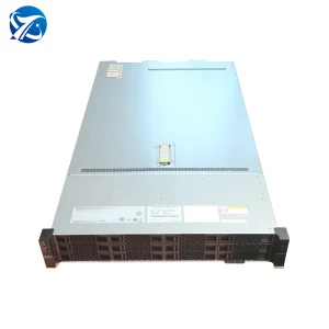
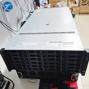
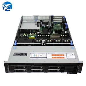
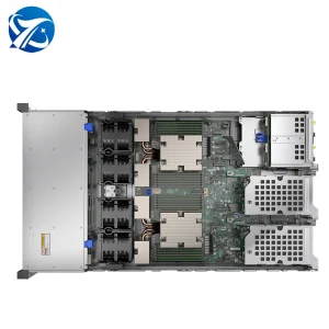
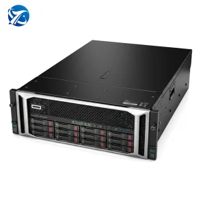
High-throughput storage interfaces and computing platforms optimized for deep integration with custom OEM architectures
How Custom microcode, chiplet technologies, and ISA personalization are transforming modern computing paradigms
The global semiconductor landscape is undergoing a massive shift from general-purpose processing to highly specialized, application-specific architectures. While standardized x86 CPUs have dominated the enterprise and data center markets for decades, the rise of intense AI computing, complex machine learning workloads (such as DeepSeek optimization), and edge infrastructure requires deeper architectural flexibility. Enterprises are discovering that traditional off-the-shelf CPUs present performance bottlenecks and efficiency losses under sustained specialized workloads.
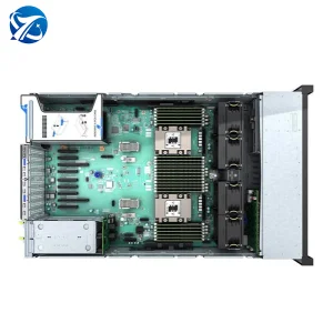
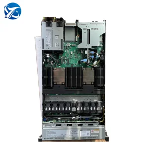
Today, OEM CPU customization lies at the heart of hardware optimization. Industry leaders leverage chiplet architectures to mix and match computing cores, on-die memory (such as High Bandwidth Memory, or HBM), and specialized AI accelerators within a single CPU package. This modular approach allows custom OEM manufacturers to adapt processors directly to customer computational targets, enabling superior instructions-per-clock (IPC) scaling for specific algorithms without driving up system-wide thermal envelopes.
Concurrently, open instruction set architectures like RISC-V and power-efficient configurations on ARM are challenging traditional x86 hegemony in server and network infrastructure. Custom instruction additions, dedicated cryptographic engines, and tailor-configured L1/L2/L3 caches are now common requests from cloud service providers (CSPs) and hyperscalers. By leveraging specialized OEM CPU custom design, organizations can strip away redundant generic processing circuits, saving critical silicon area and translating directly into significant cost savings at the utility scale.
As we advance into the sub-3nm fabrication nodes, the synergy between hardware customization and software compilation becomes the primary driver of performance gains. This co-design strategy guarantees that key computing layers (like matrix multiplication for AI training and model inference) bypass legacy compute cycles, achieving unparalleled throughput and securing a definitive technology advantage in highly competitive computing markets.
Combining diverse instruction set architectures, integrated high-speed memory modules, and task-specific hardware accelerators on a single multi-chip module (MCM) to maximize computing density.
Developing hardware-level cryptographic accelerators, memory encryption layers, and physically unclonable functions (PUF) directly within custom processor microcode.
Fine-tuning micro-architectural execution units, branch prediction tables, and out-of-order execution logic to accelerate target software libraries, specifically AI mathematical frameworks.
Navigating capital allocation, design complexity, thermal envelope boundaries, and long-term hardware reliability metrics
Custom OEM processors require robust thermal profiling to thrive in densely packed enterprise enclosures. By matching CPU target TjMax, thermal resistance values, and integrated heat spreader (IHS) materials to specific data center cooling setups (whether advanced liquid cooling loops or high-airflow fan arrays), procurement managers can avoid performance throttling and ensure steady-state operations.
Enterprise procurement teams prioritize hardware security. Custom OEM processors allow for bespoke microcode configurations that disable unused internal diagnostic interfaces, preventing physical and side-channel threats. Additionally, custom security micro-kernels can be flashed at the factory floor level to maintain a strict, chain-of-trust boot process across global installations.
Every watt matters in modern computing. Tailored CPUs eliminate power-hungry, redundant logic gates to lower the overall thermal design power (TDP). This reduction lowers the active power draw of the chip and eases system cooling requirements, generating measurable, multi-million dollar utility savings when deployed across massive server footprints.
Public clouds and industrial operations cannot tolerate sudden end-of-life cycles. Procuring through dedicated OEM CPU exporters ensures long-term hardware availability, guarantees standard microcode security updates, and provides structured component replacement pathways that span a decade or more, far outpacing the typical lifespans of retail-grade silicon.
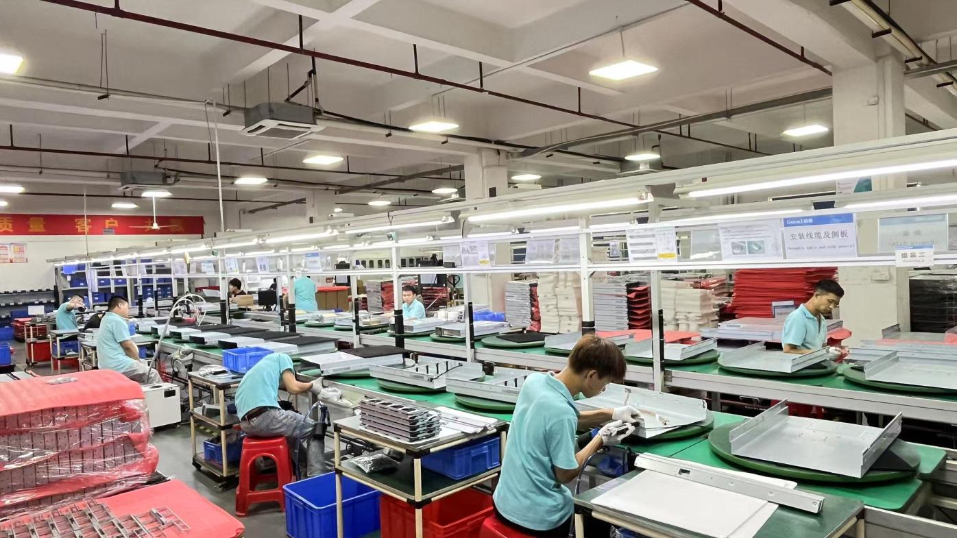
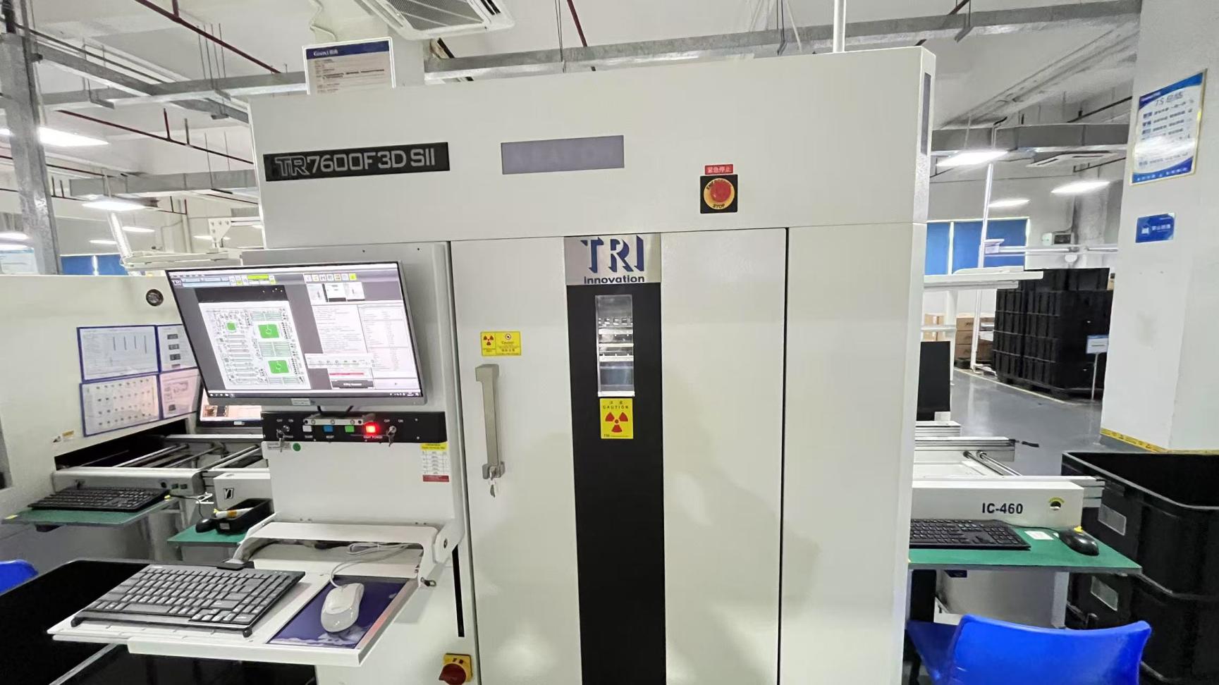
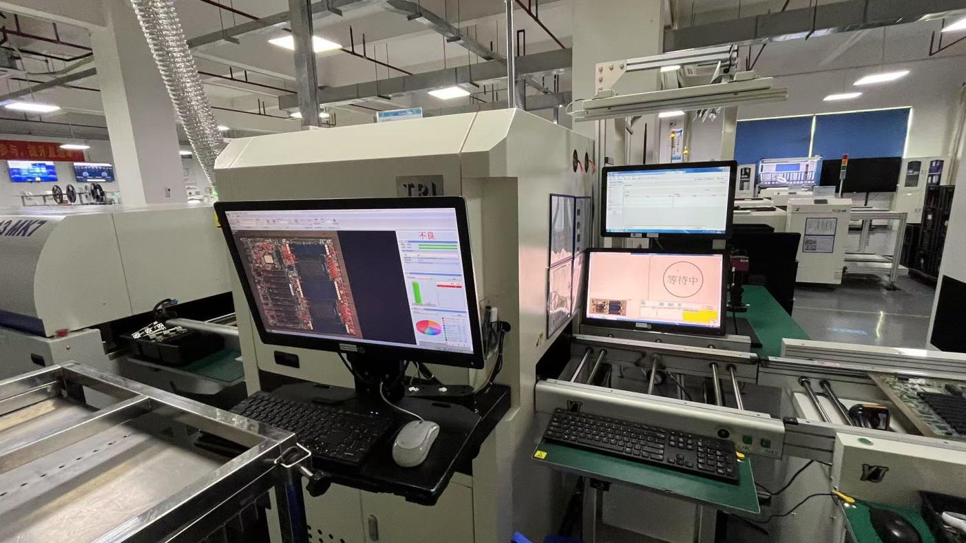
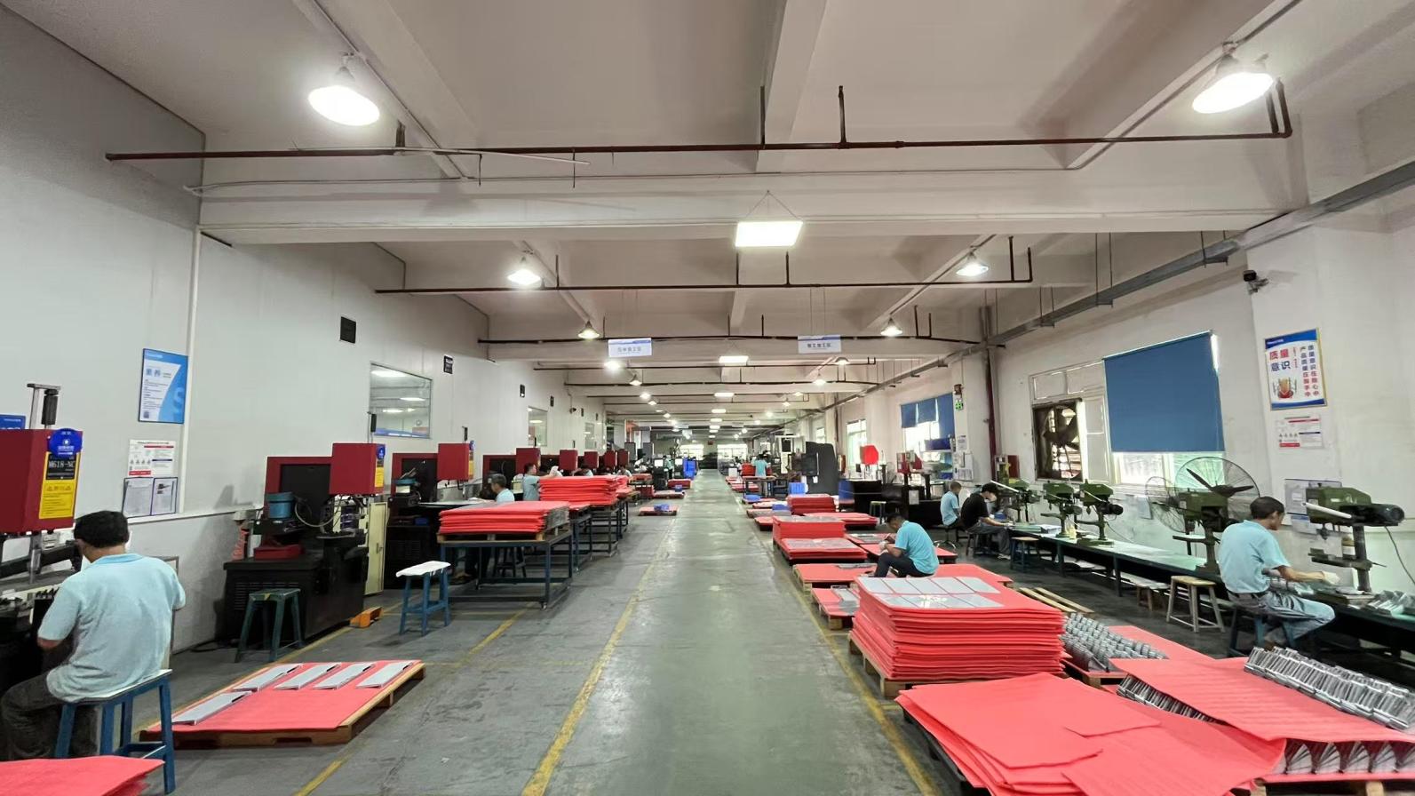
China's modern manufacturing facilities have shifted from basic volume assembly to advanced Factory 4.0 methodologies. Characterized by real-time automated visual inspection, AI-driven precision surface-mount technology (SMT) lines, and automated silicon performance binning, Chinese manufacturing plants offer unmatched supply chain resilience and design adaptability.
NexaGPU stands at the forefront of this industrial evolution, specializing in high-performance computing configurations, complex GPU clusters, and highly customized server integrations for enterprise applications globally. By working with a deep ecosystem of over 850 supply chain partners, NexaGPU guarantees immediate component availability, robust pricing, and fast hardware validation cycles.
Rather than managing production in monolithic, slow-moving mega-factories, NexaGPU leverages an agile, highly specialized 320m² state-of-the-art testing and integration facility. Supported by 120 dedicated R&D engineers and 45 specialized quality control (QC) experts, this specialized assembly and validation environment allows NexaGPU to prototype, test, and release 85 new product configurations in a single calendar year, maintaining rapid speed-to-market and high operational quality.

Mapping customized CPU configurations to compute workloads, environments, and business scenarios
For modern datacenters running large-scale language model inference (such as DeepSeek R1 networks), customized PCIe bus routing, increased memory channels (DDR5/HBM3), and tailor-fit Intel Xeon configurations ensure maximum data transfer speed and low latency between host processors and massive GPU clusters.
Remote edge nodes must perform reliably under strict power limits and high-temperature environments. Standard commercial chips struggle in these spaces. Custom OEM CPUs address these constraints by lowering TDP, omitting unneeded execution units, and extending operating thermal tolerances to ensure stable operations inside sealed, fanless outdoor enclosures.
In high-frequency trading, microseconds decide profitability. Generic processors incur latency through standard branching operations and safety protocols. Custom OEM microcode optimizations enable financial engines to bypass non-essential checks, run direct execution paths, and maximize single-thread frequencies, securing a decisive performance edge.
Expert technical insights detailing customized CPU validation, supply chains, microcode modification, and system thermal management
Custom CPU MOQs scale according to the depth of physical silicon customization required. Minor adjustments, such as microcode tuning, custom validation profiles, or applying specialized integrated heat spreaders (IHS), typically require 100 to 500 units per production run. Deep architectural changes, such as multi-chip module (MCM) package adjustments, customized substrate designs, or dedicated silicon fabrications, require larger runs (often 5,000+ units) to offset the primary non-recurring engineering (NRE) costs.
Our specialized validation team employs a rigorous multi-stage testing sequence. Hardware is subjected to intensive high-load burn-in testing, cyclic thermal stress testing inside environmental chambers, and high-frequency voltage fluctuation testing to check power delivery health. Every system must pass extensive error-correcting code (ECC) memory tests and raw computational diagnostics under extreme workloads (such as continuous, high-concurrency model execution loops) before shipping.
Yes. On ARM-based architectures (under custom licensing agreements) and open RISC-V configurations, we collaborate directly with design houses to integrate custom execution units. These units accelerate target software processes, such as vector processing, tensor math, or proprietary hash functions. We also provide complete toolchain support to ensure your software compilers can easily leverage these hardware-level optimizations.
Typical timelines depend on customization depth:
• Stage 1: Design Phase (2 - 4 weeks) – Technical discovery, microarchitectural modeling, and simulation.
• Stage 2: Prototyping (4 - 6 weeks) – Silicon validation (for simple modifications) and producing prototype boards.
• Stage 3: Validation & Quality Control (3 - 5 weeks) – Extensive stress tests, thermal profiling, and system-level validation.
• Stage 4: Production & Delivery (4 - 8 weeks) – SMT lines, validation runs, and air/ocean shipping logistics.
Custom CPU configurations allow us to run processors at lower target core voltages by disabling unused logic blocks and fine-tuning clock profiles. This step can reduce active power consumption by up to 25% compared to off-the-shelf equivalents, significantly reducing active heat output and simplifying server chassis design. The resulting reduction in thermal stress translates to lower fan requirements and quieter, more cost-effective datacenter operations.
Scalable computational platforms featuring advanced custom multi-socket processors and GPU acceleration layers